
FAQ
13. Everlast Win capacity per month?
14. The advantages of Immersion Gold?
♦ Good adhesion and is well-known for its electrical testability as well.
♦ Good plating around the holes in the circuit board.
♦ Gold wire bondable, and can be soldered easily.
♦ Best for fine pitch products because the tracks or pads are square-edged and flat.
♦ All RoHS requirements.
15. What are the impacts of transition from HASL to Lead Free HASL?
In Lead Free HASL, the operating temperature of wave soldering is up to 270°C to cause heat impact on substrates. If the heat or acid resistance of the solder mask is low, soldering folds, side corrosion, or grid peeling are the common anomalies.
2. In HASL, folds are often found in vias to cause poor hold blocking. In addition, PCB cracking from thermal expansion also occurs if dedicated via mask is not used or drying is inadequate. Therefore, it is very important to choose heat-resistant masks and correct hole blocking methods.
3. Substrate
Select substrates of medium to high Tg, and pay attention to the coefficient of thermal expansion (CTE).
4. Surface Cleanliness
Lead Free HASL operating at high temperatures can easily cause the evaporation or cracking of the organic compounds in the flux to lose the facilitation and wetting functions. Eventually, solder spattering will take place on the substrate or solder mask. Therefore, select flux with high viscosity. Although heat resistance and wetting are enhanced, the probability of false soldering or non-wetting also enhances.
5. Coating
When operating at high-temperature furnaces, lead-free solders have higher fluidity, particularly in vertical HASL/HAL. Due to surface tension, solders will deposit at a particular point to result in uneven coating. The specific gravity of lead-free vs. leaded solders is 7.5 vs. 8.4. As the specific gravity reduces, cohesive force and surface tension increase to reduce pad smoothness.
6. Higher Risk for Rework
The probability of the following will enhance: Thickening of the intermetallic compound (IMC) layer, via copper etching, solder heat resistance, loosening of independent pads and fiduciary marks, board cracking or via cracking.
16. The advantages and disadvantages for OSP (Organic Solder-ability Preservatives)?
Disadvantages: No way to measure thickness, not good for PTH, short shelf life, can cause ICT issues, exposed Cu on final assembly and handling sensitive.
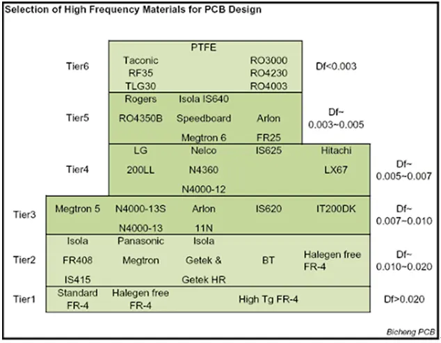
17. What are the effects of Dk and Df of substrates ?
If the permittivity of the insultation materials in a multilayer board is higher, much of the energy for signal transmission has been stored in the materials. This will result in poor “signal integrity” and low “signal transmission rate.” Therefore, the lower the Dk of insulation materials, the better the quality of signal transmission. Currently, the best Dk value at 2.5 is found in PTFE boards at 1MHz, while the Dk value of FR4 boards is about 4.5.
2. Df (dissipation factor)
Df refers to the ratio between the signal energy loss in the insulation materials and residual energy in the wire. To facilitate HF signals to fly out of the PCB into the air, the lower the Df of the PCB, the better. By contrast, the higher the Df is, the poorer the signal quality is of RF communication products. In addition, the higher the frequency is, the lower the board Df should be. Like the case of a flight taking off, the taxiing runway should be very robust to reduce energy dissipation.
18. Everlast Win Line width/space capability?
| Inner | Mini width/space (Cu. 0.5oz) | 2.5mil / 2.5mil |
| Mini width/space (Cu. 1oz) | 2.5mil / 3mil | |
| Mini width/space (Cu. 2oz) | 4mil / 6mil | |
| Mini width/space (Cu. 3oz) | 5mil / 8mil | |
| Mini width/space (Cu. 4oz) | 6mil / 10mil | |
| Outer | Mini width/space (Cu. 1oz) | 3mil / 3mil |
| Mini width/space (Cu. 2oz) | 4mil / 6.5mil | |
| Mini width/space (Cu. 3oz) | 5mil / 8.5mil | |
| Mini width/space(4oz) | 6mil / 10.5mil |
19. Does EW provide urgent trial order service?
20. If EverlastWin could support “Backdrill”?
diameter than the PTH to remove the conductive plating or stub from the hole. In practice this is
achieved by re-drilling the PTH down to a predetermined stub length less than 10 mils from the signal
layer.
Advantages:
• Reduced deterministic jitter
• Less signal attenuation with improved impedance matching
• Minimal design and layout impact
• Reduced via-to-via crosstalk
• Lower costs than sequential laminations
21. What is a high-speed PCB material?
A high-speed PCB is a circuit board having a digital circuit speed at or above 45 to 50MHZ, and digital circuit signals account for more than one-third of the entire system.
In fact, high-speed PCBs do not have an authoritative definition. Back in the 1960s, when digital electronics began developing, the signal speed was low, and PCB design could be done without much effort. Later, the digital circuit signal speed elevates, and engineers find that traditional PCB designing doesn’t work for these high-speed circuits, so they optimize the circuit design and use specific PCB base materials. The PCBs developed for these high-speed circuits are called high-speed PCBs. But no specific signal speed value is defined for speed-speed values, and no necessity to do it.
High-speed PCB mainly use in GPS receiver, mobile, RF, Radar…etc.
| Rogers RO3003 |
Rogers RO3006 |
Rogers RO3001 |
ARLON 85N |
ISOLA IS620 E Ceramic |
Taconic RF-35 Ceramic |
Taconic TLX | |
| g | – | – | 160° | 250° | 220° | 315° | – |
| CTE | 25 | 24 | – | 55 | 55 | 64 | 135 |
| Electric Strength | – | – | 98 | 57 | – | – | – |
| Surface Resistivity | 1×10^7 | 1×10^5 | 1×10^9 | 1.6×10^9 | 2.8×10^6 | 1.5×10^8 | 1×10^7 |
| Thermal Conductivity | 0.5 | 0.79 | 0.22 | 0.2 | – | 0.24 | 0.19 |
| Dk | 0.0013 | 0.002 | 0.003 | 0.0100° | 0.008 | 0.0018** | 0.0019 |
| Td | 500° | 500° | – | 387° | – | – | – |
| Peel Strength | 2.2 | 1.2 | 2.1 | 1.2 | 1.2 | 1.8 | 2.1 |
22. What is PCB material utilization?
23. What is the best utilization for the PCB layout?
By consulting with them early, you can avoid annoying and costly redesigns to fix these manufacturing problems, as well as getting the most efficient panel design possible.
24. What are panelizationdetails that PCB designers should consider?
Components like connectors that overhang the boardwill require extra clearance room around the board outline in the panel. This could impact the design of the panel, and you should consult with your manufacturer to explore all the options first.
♦ Tooling Holes and Fiducial Marks:
Your manufacturer will be including these features in the panel, and you will want to make sure that your placement doesn’t cause any problems.
♦ Component Weight:
Large concentrations of components can cause the panel to bend, which would necessitate additional support. By first consulting with your manufacturer, you can find out if there are any PCB layout options that can help.
♦ PCB Width:
In the same way, thin circuit boards could also cause a panel to bend. This can lead to problems such as solder coming over the top of some of the boards as the panel bends going through the wave. This may result in your manufacturer having to brace the board or use a pallet, which could have an impact on how you place your components.