
PCB Process - Back Drill
PCB Process - Back Drill
I. What is PCB “Back Drill”?
Back drill is actually a special type of drilling for the hole depth. In the multilayer production, take a 12 layer board as an example, we need to connect the 1st layer to 9th layer. Usually, we drill a through hole and then sink the copper. In this way, the 1st layer is directly connected to the 12th layer; however, in fact, we only need to connect the 1st layer to the 9th layer. Since there is no wire connection from the 10th layer to 12th layer, it’s like pillar.
This pillar affects the signal path leading to signal integrity issues in communication signals. We drill an additional pillar from the opposite side (secondary drilling) and it’s called back drill.
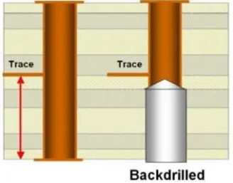
Left: it shows a normal signal through-hole.
Right: it shows a schematic diagram of a through-hole after back drilling, indicating it is drilled from the bottom layer to the signal layer where the trace is located.
II. Why do we need a back drill design?
The through holes of PCBs are usually designed as vias (from the top layer to the bottom layer). When the traces connecting the vias are closed to the top layer, a “stub” fork will be generated at the via in the interconnection of the PCB, which will cause signal reflection and affect the quality of the signal. This impact is greater for high speed signals, so it is necessary to remove the stubs of the vias on the PCB. “Back drill” is a PCB processing technology used to achieve this purpose.
What are the advantages of the back drill?
1. Reduce noise interference.
2. Improve signal integrity.
3. Reduce partial board thickness.
4. Reduce the use of the blind holes and the difficulty of the PCB production process.
III. What is the function of the back drill?
The function of the back drill is to remove the portion of the via that has no connection or transmission function to avoid reflection, scattering and delay in high-speed signal transmission which may cause distortion to the signal. It indicates that the main factor impacts the signal integrity of the signal system is design, board material, transmission line, connector, chip…etc. There’s no doubt the vias have a great influence on the signal integrity environment.
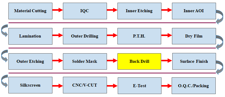
IV. Back Drill Flow Chart
V. What signal speeds require the back drill technology?
- In general: signals with speeds ≥5Gbps should consider the back drill design.
- If the chip’s driving capability is strong enough or the system interconnection links are not long, it may be possible to pass the signal quality without back drill design.
Remark: Any communication links consist of three parts: transmitter (TX), medium (message channel) and receiver (RX).