
What is a Printed Circuit Board
What is a Printed Circuit Board?
A Printed Circuit Board (PCB) is a Sheet of Insulating Material such as Fiberglass, with Metallic Circuit or Track Printed or Etched on it for Electrical Conductivity. A PCB is found in almost all electronic products that we use in our daily life – Mobile Phone, Tablet, TV, Computer, Laptop, Keyboard, Mouse, Military Weapons, Airplane, Satellite etc.
Alternatives to PCBs include wire wrap and point-to-point construction, both once popular but now rarely used. PCBs require additional design effort to lay out the circuit, but manufacturing and assembly can be automated. Electronic design automation software is available to do much of the work of layout. Mass-producing circuits with PCBs is cheaper and faster than with other wiring methods, as components are mounted and wired in one operation. Large numbers of PCBs can be fabricated at the same time, and the layout has to be done only once. PCBs can also be made manually in small quantities, with reduced benefits.
1. PCB Material
The base of a PCB can be made with different material. The condition is that the material should be heat resistant, insulating and durable. The base material of a PCB (CCL – Copper Clad Laminate) is basically composite material made of dielectric layer (Resin, Glass Fiber) and conductor or high purity (copper foil).
Commonly used materials to make PCBs are:
- FR-4: a woven fiberglass cloth impregnated with an epoxy resin. Low water absorption (up to about 0.15%), good insulation properties, good arc resistance. Very common. Several grades with somewhat different properties are available. Typically rated to 130 °C. Operation environment is high temperature, recommend the High Tg FR-4.
- High Tg FR-4:glass fiber and epoxy. Typically rated to Tg150 °C means High Tg.
- CEM-1:cotton paper and epoxy.
- CEM-3:non-woven glass and epoxy.
- Ceramic PCB:Ceramic and glass fiber.
- Teflon PCB:Teflon and glass fiber.
2. PCB Surface Finishes
A surface finish is essential for making a reliable connection between the PCB and the electronic component. A surface finish has two major functions, to provide a solderable surface for sufficient soldering components to the PCB, and to protect any exposed copper from oxidizing.
7 Types of PCB Surface Finishes:
- Bare Copper Board:
The traces inside the board is mainly pure copper, that is, bare copper board.
Advantages:
Low cost, flat surface, good solderability.
Disadvantages: It’s easy to be affected by acid and humidity. It cannot be stored for a long time, after unpacking need to be used up within 2 hours because the copper is exposed to the air easily oxidized.
- Hot Air Solder Leveling(HASL/HAL):
It is widely available and very economical. The board is dipped in molten solder and then leveled off with a hot air knife. If you’re using through-hole or larger SMT components, HASL can work well.
The surface is not completely level, so this can cause issues with small components. The solder used is typically Tin-Lead. That means that it isn’t RoHS compliant. And if reducing the amount of lead you use is important, you may want to choose Lead-Free HASL instead.
- Lead-Free HASL:
Lead-Free HASL is similar to standard HASL, but with an obvious difference… It doesn’t use Tin-Lead solder. Besides, like standard HASL it is not ideal for smaller components.
For boards with smaller components, immersion coatings can be a better choice. They are slightly more expensive but more suitable for this purpose.
- ENIG (Electroless Nickel Immersion Gold):
Electro gold flash plating consists of a thin layer of gold over electroless or electrolytic nickel. This type of plating is hard and durable. It also has a long shelf life, lasting for years. However, its durability and shelf life make it more expensive than any of the finishes mentioned above.
- Gold Plating:
Gold is real gold. Even if a very thin golden layer will account for nearly 10% of the cost of the circuit board. Using gold as a plating layer is one for facilitating soldering and the other for preventing corrosion. The gold-plated layer is widely used in the component pads, gold fingers, connector shrapnel, and other positions of the printed circuit board.
- Immersion Silver:
Immersion silver is a non-electrolytic chemical finish applied by immersing the copper PCB into a tank of silver ions. It is a good choice finish for circuit boards with EMI shielding and is also used for dome contacts and wire bonding. The average surface thickness of the silver is 5-18 micro inches.
With modern environmental concerns such as RoHS and WEEE, immersion silver is environmentally better than both HASL and ENIG. It is popular also due to its lesser cost than ENIG.
- OSP(Organic Solderability Preservative):
OSP is the abbreviation of organic soldering film. It used organic in surface finish but not metal, leading to a cheaper price than HASL.
The only function of this organic film is to ensure that the inner copper foil will not be oxidized before soldering. This layer of film volatilizes as soon as it is heated during soldering and solder the copper traces and the components together. But OSP is not resistant to corrosion. If an OSP circuit board is exposed to the air for ten days, the components cannot be soldered.
Many computer motherboards use OSP technology. Because the area of the circuit board is too large, it is expensive for using immersion gold.
3. Types of PCB
- Single-sided PCB:
Single sided printed circuit boards are circuit boards with one layer of conducting material on one side of the board, while the other side is used for incorporating different electronic components.
A single sided board is made of a substrate layer, a conductive metal layer and followed by a protective solder mask and silk screen. Single sided circuit boards were the first printed circuit board technology and have been in circulation since the 1950s, and remain one of the most commonly used circuit boards due to their simple design.
- Double-sided PCB:
Double-sided PCBs are the same as single-sided PCBs, but the difference is they have two sided traces with a top and bottom layer. Double-sided PCBs can mount conductive copper and components on both sides of the printed circuit board so that the traces can cross over each other. It leads to a higher density of boards without the need of point-to-point soldering. It’s difficult to fabricate the double-sided PCBs because they are more complex than single-sided PCBs.
Double-sided PCBs are one of the most popular types of PCBs because they make manufacturers to fabricate more complex circuits, which can benefit uses in higher technology applications and electronics.
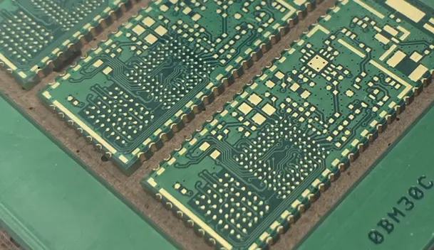
- Multi-Layer PCB:
Multilayer PCBs can support a high level of circuit complexity as they are made up of three or more copper layers laminated together. And the manufacturer begins to use a core that has the same materials as a typical single-sided or double-sided PCB. After etching the inner core, they add a layer of prepreg, a soft fiberglass, which remains the layers together and be the hard fiberglass after the board goes through a hot press. So multilayer PCBs are durable and tough after the curing process. Needless to say, it will use one core, prepreg and copper foil for the top and bottom layers if the manufacturer is fabricating a 4 layer PCB.
There are complex technologies like computers and data servers because of the high capacity of multilayer PCBs.
4. PCB Material
- FR-4
FR4 is a class of printed circuit board base material made from a flame retardant epoxy resin and glass fabric composite. FR stands for flame retardant and meets the requirements of UL94V-0. FR4 has good adhesion to copper foil and has minimal water absorption, making it very suitable for standard applications. FR4 is either used as a copper-coated material for 1 and 2-layer PCBs or is used for multilayer PCBs as a Prepreg and core.
- PTFE
Teflon PCB, or PTFE PCB, is a high-frequency PCB using polytetrafluoroethylene (PTFE) as its PCB substrate. Teflon PCBs transmit signals of 5GHz and higher frequencies. Teflon is the brand name that Dupont Corporation uses for its PTFE materials, and it is so well-known that people use Teflon PCB to refer to PTFE substrate PCBs used for microwave and RF applications. There are quite a few Teflon PCB models in the market, and Teflon PCB material suppliers include Rogers, Taconic, Taizhou Wangling, Nelco, and Arlon. All Teflon PCBs have these advantages:
˙ Low signal delay and electrical loss due to small DK and Df
˙ Stable signal transmission over a wide frequency range due to small TDK
˙ Low moisture absorption
˙ High reliability due to low CTE The above advantages of Teflon PCBs clearly tell us that Teflon PCBs are specially used in high-frequency fields.
- Alumina (Ceramic)
Ceramic PCB or calls Alumina PCB is a kind of heat conducting ceramic powder and organic binder which is a printed circuit board with high thermal conductivity and a low expansion coefficient (CTE), the ceramic raw material are almost based on Alumina (Al2O3), Aluminum Nitride (ALN), or Beryllium Oxide (BeO).
Ceramic PCB features thermal conductivity that is more than 90 times of that of epoxy glass fiber, leading to excellent conduction cooling, which can make a quick effect on transferring heat away from hot spots and dissipating it over the whole surface. Moreover, components on ceramic PCBs usually feature a lower junction temperature (Tj) than that on ordinary PCBs.
- Aluminum
An aluminum PCB has a layer or layers of copper, solder mask and silkscreen layered over it. Instead of having a fiberglass or plastic substrate, though, an aluminum circuit board has a metal substrate. This base mainly contains a combination of aluminum. The metal core can consist entirely of metal or have a combination of fiberglass and aluminum. Aluminum PCBs typically are single sided, but can be double sided as well. Multilayer Aluminum PCBs are highly difficult to manufacture.
Aluminum boards get the most use in LED and power converting electronics. The intense light produced by LEDs creates high levels of heat, which aluminum directs away from components. An aluminum PCB extends the lifespan of an LED device and provides more stability. You can find aluminum substrates in street lights, stop lights and household lighting.
- Others:FR series like FR-3, FR-5, FR-6 and CEM series like CEM-1 ~ CEM-5.
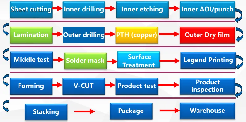
5. PCB Manufacture Process
6. Types of Drilling
- Mechanical Drilling:
Using mechanical drilling is that the tool creates very high-quality holes that are consistent in nature no matter the number of holes that are drilled. The holes do not have a taper at the ends, they are drilled through the substrate complete leaving the knee of the wall clean with no bevel; the surface edge has a sharp finish. Another advantage is that mechanical drilling has a faster drill speed than other methods, allowing for increased through put for production quantities.
The minimum drill we could make is 0.2mm and most of through holes are made by the mechanical drilling.
- Laser Drilling:
It is the process of creating thru-holes, referred to as “popped” holes or “percussion drilled” holes, by repeatedly pulsing focused laser energy on a material. The diameter of these holes can be as small as 0.076~0.1mm. More and more HDI use the laser drilling to meet blind/buried via request.
- PTH / NPTH
Plated Through Holes (PTH) are PCB features that are either milled or drilled, and then plated afterwards with conductive copper. By running traces between the plated through holes, components soldered in those positions are then electrically connected to other components on the circuit board.
Non-plated Through Holes (NPTH) are simple features that are either drilled or milled through your circuit board, which expressly do not receive a plating of conductive copper. Typical uses of NPTH features are mounting holes to allow screws or other fasteners to pass through your board.
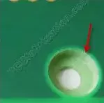
- Blind/Buried via:
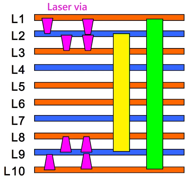 Blind via (pink color): A blind via connects an outer layer of the board to inner layers and doesn't go through the entire board.
Buried via (yellow color): A buried via connects inner layers without reaching the outer layers.
Both blind and buried vias do go all the way through from top to bottom. Blind buried vias provide electrical connections from the outer layers to the inner layers as well as in between the inner layers and are used when you have limited space on your PCB. You mostly see blind and buried vias in High density interconnect (HDI) PCBs. HDIs provide benefits such as increased layer density, improved power delivery and use of much smaller pitch devices. The hidden vias help keep the board light and compact. It is common to see blind and buried vias in electronic products like, cell phones, laptops, and medical devices.
- Plated Half Hole (Castellation):
It also called castellated holes, which is plated with copper based on the specialized process on the edge of PCB. Plated half-holes are predominantly used for board-on-board connections, mostly where two boards with different technologies are combined. Plated half holes boards are applied to industries such as: telecommunication, computer application, industrial control, power, automobile and high-end consumer electronics, and so on.
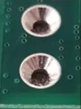
- Countersink / Counterbore:
A countersink (left) produces a conical hole matching the angle of the screw so that when the screw is fully engaged the head will sit flush or slightly below the surface. A counterbore (below) is used to enlarge the opening of a hole producing a flat bottom so a socket-head screw will fit flush with the surface of the part. The chamfer angles of a countersink typically are either 82, 90, 100, 110 or 120 degrees.
-
 Countersink
 -
 Counterbore
7. Special Types of PCB
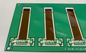
- Flexible Printed Circuit Board
Flexible Printed Circuit (FPC) is a technology developed by the United States for the development of space rocket technology in the 1970s. It is made of polyester film or polyimide as a substrate with high reliability and excellent flexibility. By embedding a circuit design on a flexible thin plastic sheet, a large number of precision components can be stacked in a narrow and limited space to form a flexible circuit. This kind of circuit can be bent at will, folded, lightweight, small size, good heat dissipation, easy installation, and breaks through the traditional interconnection technology. In the structure of the flexible circuit, the materials are insulating film, conductor, and adhesive. Flexible Printed Circuits are the only solution to meet the miniaturization and mobile requirements of electronic products. Flexible printed circuits can greatly reduce the volume and weight of electronic products and are suitable for the development of electronic products in the direction of high density, miniaturization, and high reliability.
- RFPCB (Rigid-Flex Printed Circuit Board)
 Rigid-Flex printed circuit boards are boards using a combination of flexible and rigid board technologies in an application. Most rigid flex boards consist of multiple layers of flexible circuit substrates attached to one or more rigid boards externally and/or internally, depending upon the design of the application. The flexible substrates are designed to be in a constant state of flex and are usually formed into the flexed curve during manufacturing or installation.
Rigid-Flex PCBs offer a wide array of applications, ranging from smart devices to cell phones and digital cameras. Increasingly, rigid-flex board fabrication has been used in medical devices such as pacemakers for their space and weight reduction capabilities.
8. PCB Certification
- UL
Underwriter Laboratories (UL) is one of the oldest safety certification companies around. They certify products, facilities, processes or systems based on industry-wide standards. By doing so, they issue over twenty different UL Certifications for a wide-range of categories. Certain UL Marks are country specific and will never be used or seen in the United States and vice versa. There is no such thing as general UL approval, instead they break up their certification into being listed, recognized, or classified.
UL Listed Service is given to manufacturers that produce products that meet UL’s standards and gives the manufacturer authorization to test products and apply the UL mark themselves.UL Recognized Serviceis applied to products used to produce another product, which indicates that it is safe to use in further production and it is not a mark that is seen on an end product.
UL Classification Service can be placed on products by a manufacturer that makes products that comply with UL’s standards and maintains follow-up with UL to ensure quality and accuracy.
- ISO 9001
ISO 9001 is defined as the international standard that specifies requirements for a quality management system (QMS). Organizations use the standard to demonstrate the ability to consistently provide products and services that meet customer and regulatory requirements. It is the most popular standard in the ISO 9000 series and the only standard in the series to which organizations can certify.
ISO 9001 was first published in 1987 by the International Organization for Standardization (ISO), an international agency composed of the national standards bodies of more than 160 countries. The current version of ISO 9001 was released in September 2015.
- ISO 14001
ISO 14001 is the international standard that specifies requirements for an effective environmental management system (EMS). It provides a framework that an organization can follow, rather than establishing environmental performance requirements.
Part of the ISO 14000 family of standards on environmental management, ISO 14001 is a voluntary standard that organizations can certify to. Integrating it with other management systems standards, most commonly ISO 9001, can further assist in accomplishing organizational goals.
The International Organization for Standardization (ISO) defines an environmental management system as “part of the management system used to manage environmental aspects, fulfill compliance obligations, and address risks and opportunities.” The framework in the ISO 14001 standard can be used within a plan-do-check-act (PDCA) approach to continuous improvement.
- IATF 16949
IATF 16949 is a global Quality Management System Standard for the Automotive industry. IATF 16949:2016 incorporates the structure and requirements of the ISO 9001:2015 quality management system standard with additional automotive customer-specific requirements. It was developed by the International Automotive Task Force (IATF), with support from AIAG. This standard requires certification by a 3rd party auditor (Registrar/CB/Certification Body). Here are some key areas of focus:
- Continuous improvement
- Defect prevention
- Reducing waste
- Product safety
- Risk management
- Contingency planning
- Requirements for embedded software
- Change and warranty management
- Management of sub-tier suppliers
- “IATF 16949 Certified” means an organization has met the requirements in IATF 16949.
- RoHS
RoHS is a product level compliance based on the European Union's Directive 2002/95/EC, the Restriction of the Use of certain Hazardous Substances in Electrical and Electronic Equipment (RoHS). Products compliant with this directive do not exceed the allowable amounts of the following restricted materials: lead, mercury, cadmium, hexavalent chromium, polybrominated biphenyls (PBB) and polybrominated diphenyl ethers (PBDE), with some limited exemptions.
This directive applies to manufacturers, authorized representatives, importers and distributors of products including large household appliances (refrigerators, etc.), small household appliances (vacuum cleaners, etc.), computing & communications equipment, consumer electronics, lighting, power tools, toys and sports equipment and automatic dispensers (ATM machines).
Organizations often prove RoHS compliance with a letter of compliance issued by an employee of the company. There are third party testing services available that will test an organization's products for levels of the restricted materials.
- REACH
REACH is a European Regulation and is an acronym for the Registration, Evaluation, Authorisation and Restriction of Chemicals. The overall aims of REACH are to:
- 1. Provide a high level of protection of human health and the environment from the use of chemicals
- 2. Allow free movement of substances on the EU market
- 3. Enhance innovation and the competitiveness of the EU chemicals industry
- 4. Reduce animal testing by promoting the use of alternative methods of assessing chemicals
REACH entered into force on 1st, June 2007 and replaced a large number of European Directives and Regulations in a single system.
The main difference between RoHS and REACH is that RoHS bans substances that are present in electronics and is specific to the aforementioned 6 hazardous materials. REACH, however, pertains to all chemicals including those used to make a product. This can include materials, solvents, paints, chemicals, and more.