PCB Process - Edge Plating
PCB Process - Edge Plating

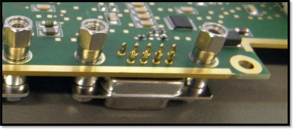
Printed Circuit Board (PCB) Edge Plating refers to the copper plating layer that extends from the TOP side to the BOT side and along one side edge of the board. In the manufacturing process, the edges that need to be metallized are subjected to CNC milling before copper plating and appropriate surface treatment is performed on the edges of the PCB after copper plating.
Design application of the edge plating on the Printed Circuit Board (PCB):
Design application of the edge plating on the Printed Circuit Board (PCB):
- Enhance Current Conduction Improving the current carrying capacity can enhance the printed circuit board (PCB) reliability and quality. In addition, the correct level of conductivity is an ideal choice for components to operate as intended, and it can protect vulnerable edge connections.
- Signal Integrity Edge plating enhances the signal integrity of printed circuit board (PCB) by preventing interference from entering the internal transmission of electrical impulses.
- Thermal Distribution Due to the metallic nature of the edge plating, they provide additional cooling surface area to dissipate heat into the surrounding air. The metal surface enhances the reliability of printed circuit board (PCB), especially when components are heat-sensitive.
- Improve EMC/EMI Performance Metalized edges allow for the escape of stray currents, preventing the generation of sporadic electric and magnetic fields. This helps in maintaining better EMC/EMI performance.
- Enhance Electromagnetic Compatibility (EMC) Edge plating enhances the electromagnetic compatibility (EMC) of multi-layer printed circuit boards.
- Prevention of electrostatic discharge (ESD) damage When handling printed circuit board (PCB), static electricity can discharge onto sensitive components. The metal surface helps in absorbing static electricity, thereby preventing electrostatic damage.

