
PCB Warpage
Causes and Improvement Methods for Printed Circuit Board (PCB) Warpage
For each printed circuit board (PCB), the causes of board bow and twist may not be the same; generally, they can be attributed to the applied stress exceeding the capability of the PCB material to withstand it. When the stress on the PCB is unevenly distributed or when the ability to resist stress varies across different areas of the PCB, board warpage and bow can occur. In severe cases, this can result in soldering defects, tombstoning, and component displacement on the surface mount technology (SMT) assembly after completion.
The causes of printed circuit board (PCB) warpage and bow are as follows:
- Uneven distribution of copper foil in each layer of the printed circuit board (PCB)
When there is uneven copper distribution in the layers of the same PCB, it can result in uneven expansion and contraction, causing imbalanced heat dissipation and absorption. In situations where the expansion and contraction are not synchronized, different stresses can lead to deformation. If the temperature of the PCB reaches the upper limit of the glass transition temperature (Tg), the PCB will start to soften, causing permanent deformation.
- Asymmetric stack-up design of the printed circuit board (PCB)
In the stack-up configuration of a PCB, it is important to ensure mutual symmetry in terms of substrate thickness, copper foil thickness, and prepreg types. This design symmetry helps to avoid variations in stress caused by different specifications, which can lead to PCB deformation due to inconsistent stress levels.
- The weight of the printed circuit board (PCB) itself can cause PCB depression and deformation.
In general, the reflow ovens use a conveyor chain to drive the forward movement of the PCB during the soldering process. The PCB is supported at both ends, causing the entire PCB to be suspended. If there are heavy components placed on the PCB or if the PCB size is excessively large, the weight of these components can cause a depression in the middle of the PCB, resulting in board warping.
- The depth and method of connecting V-Cuts in a printed circuit board (PCB).
V-Cut is a panelization method that involves cutting and separating PCBs, which can affect the structural stress of the PCB during high-temperature processes. The depth of the V-Cut indirectly impacts the structural stress of the PCB during assembly. Additionally, the number of connected panels and the direction of the fold lines also affect the support stress of the PCB for carrying components. Adding the fold lines at the shorter edges of the connected panels can reduce the stress on the PCB. However, if the total weight of the components exceeds the carrying capacity of the PCB, it can lead to depression and deformation of the PCB.
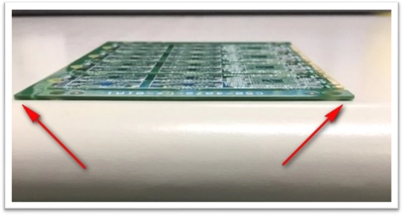
The image shows a PCB board produced using an asymmetric stack-up configuration. Even before undergoing the temperature of the assembly process, it is obvious that the board exhibits bending and warping.
The improvement methods for the printed circuit board (PCB) warpage and bow:
- Choose printed circuit board (PCB) materials with a high glass transition temperature (Tg) for production Tg (Glass transition temperature) refers to the temperature at which a material changes from a glassy
- Replace the v-cut panelization with router for the thin printed circuit board (PCB) The v-cut panelization method and the use of thinner finished printed circuit board (PCB) thickness
- Reduce the size of the printed circuit board (PCB) and minimize the number of panelization The larger the size of the printed circuit board (PCB) panel, the more prone it is to sag and deform due to its own weight during the reflow process. To minimize the sagging deformation caused by the weight of the printed circuit board (PCB), it is recommended to place the longer edge of the printed circuit board (PCB) along the conveyor chain in the reflow oven. Additionally, reducing the number of panelization is also based on the same reason. In other words, when passing through the reflow oven, it is preferable to have the shorter edge perpendicular to the direction of conveyance, in order to achieve the minimum amount of sagging deformation.
- Utilize reflow tray fixtures for components on the printed circuit board (PCB) In addition to process techniques and material selection improvements at the printed circuit board (PCB) manufacturing stage, the high-temperature expansion and subsequent cooling shrinkage of PCBs during the reflow process can be addressed by using tray fixtures in the back-end SMT assembly process. These fixtures help stabilize the printed circuit board (PCB) and, once the temperature of the printed circuit board (PCB) drops below its Tg value and begins to regain its hardness, they help maintain it original dimensions. This approach effectively reduces the issue of the printed circuit board (PCB) deformation during the reflow process.
state to a rubbery state. Choosing materials with lower Tg values means that the printed circuit board (PCB) becomes softer at a faster rate after entering the reflow process, leading to more significant deformation. Therefore, selecting the printed circuit board (PCB) materials with a high Tg value ensures that the material is more temperature-resistant, less prone to deformation, and exhibits better dimensional stability. However, it is important to note that materials with high Tg values tend to be more expensive.
(<1.2mm) can lead to deformation of the printed circuit board (PCB) after passing through the reflow process. For the thin boards, it is advisable to consider replacing the v-cut panelization method with routing or reducing the depth of v-cut. However, modifying the depth of v-cut may result in larger fiberglass burrs after board cracking, so it is necessary to evaluate whether there is any interference mechanism before implementing this change.