
Removal of Gold Finger Plating Tie Bar
Removal of Gold Finger Plating Tie Bar
Signal Integrity (SI) for High-speed PCB Design and Process of the Removal of Gold Finger Plating Tie Bar
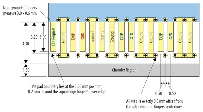
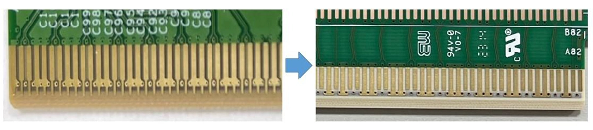
There are many factors that can affect the signal integrity of high-speed PCBs, such as insertion loss (IL), insertion loss deviation (ILD), and return loss (RL). To mitigate these factors, the first step is to determine the loss budget for the target protocol. Next, choose matching PCB materials and impedance layer design, and additional measures such as back drilling and the removal of gold finger plating tie bars can be implemented depending on the layout design requirements.Removing the Plating Tie Bar from the gold finger plating process not only prevents connector shorts caused by delamination but also ensures the reliability of the connection location. In addition, it can also improve signal integrity by reducing longer resonant stubs and parasitic capacitance, similar to the purpose of back drilling. Back drilling is used to eliminate losses in vertical signal transmission, while removing the gold finger plating tie bars is used to eliminate losses in horizontal signal transmission.
With the advent of the PCIe Gen5 interface, various PCB processes also need to be synchronized to meet the process requirements of PCIe Gen5. Therefore, the process of removing the gold finger plating tie bars has become one of the required processes for PCB manufacturers. The above photo shows Intel's latest PCIe Gen5 Layout Guide (image source: Intel website).
The gold finger pads are electroplated with hard gold through gold plating wires, and then the gold plating wires are etched away through the PCB process to reduce the signal loss of high-speed signals, thereby achieving better signal transmission.
Everlast Win Electronics Co., Ltd.