PCB Process - HDI
PCB Process - HDI
High Density Interconnect (HDI) refers to the high-density interconnect technology using the blind/buried via holes to enhance the density of circuit distributions on a PCB. The advantage is the HID can significantly increase the availability of PCB space for maximum product miniaturization. However, as circuits are densely distributed, vias cannot be drilled by traditional drilling methods, and some vias (blind) must be made by laser drilling, while buried vias must be made for interconnect.
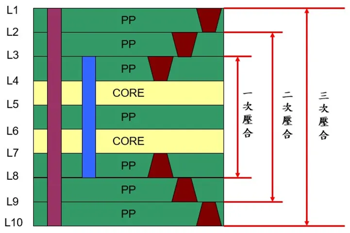
In general, the inner layers of the HDI PCB are made or laminated in advance by means of build up. After laser drilling and dimpling, the prepreg and copper foil are covered on the outer layers. Then, repeat the manufacture of circuits on the outer layers or continuously do the laser drilling to build up the layers one after another.
Usually, the laser drilling diameter is 3~4 mil (about 0.076–0.1 mm), and the prepreg thickness between layers is about 3 mil. Since the laser drilling repeats many times, the quality of an HDI PCB depends on the shape of drill vias and if the subsequent dimpling can evenly fill the vias.
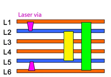
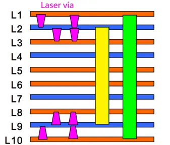
The types of HDI PCBs are as follows: the pink hole is a blind via hole made by laser drilling with diameter of 3–4 mil. The yellow hole is a buried via hole made by mechanical drilling with a minimum diameter of 6 mil (0.15 mm).
● 1+N+1
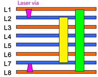
● 2+N+2
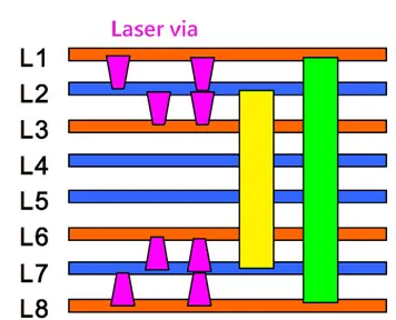
● 3+N+3